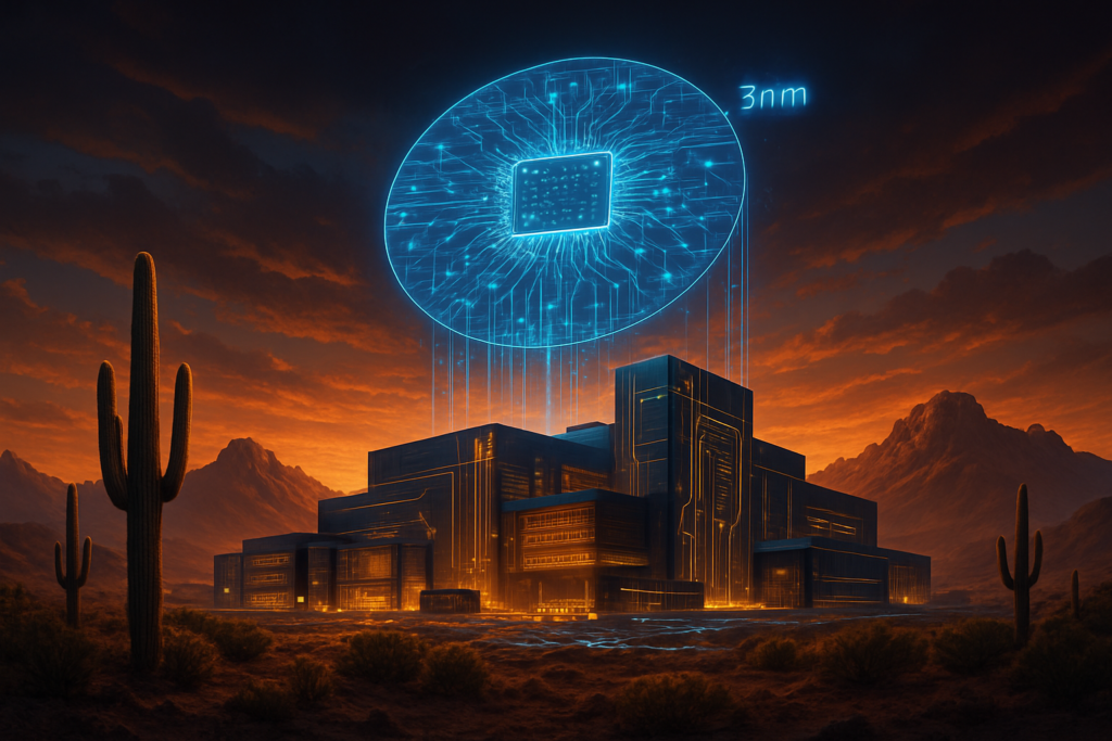
PHOENIX, AZ — In a move that fundamentally reshapes the global semiconductor landscape, Taiwan Semiconductor Manufacturing Company (NYSE: TSM) has announced a massive acceleration of its United States operations. Today, January 15, 2026, the company confirmed that its second Arizona facility will begin high-volume 3nm production by the second half of 2027, a significant pull-forward from previous estimates. This development is part of a broader strategic pivot to transform the Phoenix desert into a "domestic silicon fortress," a self-sustaining ecosystem capable of producing the world’s most advanced AI hardware entirely within American borders.
The expansion, bolstered by $6.6 billion in finalized CHIPS and Science Act grants, marks a critical turning point for the tech industry. By integrating both leading-edge wafer fabrication and advanced "CoWoS" packaging on U.S. soil, TSMC is effectively decoupling the most sensitive links of the AI supply chain from the geopolitical volatility of the Taiwan Strait. This transition from a "just-in-time" global model to a "just-in-case" domestic strategy ensures that the backbone of the artificial intelligence revolution remains secure, regardless of international tensions.
Technical Foundations: 3nm and the CoWoS Bottleneck
The technical core of this announcement centers on TSMC’s "Fab 2," which is now slated to begin equipment move-in by mid-2026. This facility will specialize in the 3nm (N3) process node, currently the gold standard for high-performance computing (HPC) and energy-efficient mobile processors. Unlike the 4nm process already running in TSMC’s first Phoenix fab, the 3nm node offers a 15% speed improvement at the same power or a 30% power reduction at the same speed. This leap is essential for the next generation of AI accelerators, which are increasingly hitting the "thermal wall" in massive data centers.
Perhaps more significant than the node advancement is TSMC's decision to build its first U.S.-based advanced packaging facility, designated as AP1. For years, the industry has faced a "CoWoS" (Chip on Wafer on Substrate) bottleneck. CoWoS is the specialized packaging technology required to fuse high-bandwidth memory (HBM) with logic processors—the very architecture that powers Nvidia's Blackwell and Rubin series. By establishing an AP1 facility in Phoenix, TSMC will handle the high-precision "Chip on Wafer" portion of the process locally, while partnering with Amkor Technology (NASDAQ: AMKR) at their nearby Peoria, Arizona, site for the final assembly and testing.
This integrated approach differs drastically from the current workflow, where wafers manufactured in the U.S. often have to be shipped back to Taiwan or other parts of Asia for packaging before they can be deployed. The new Phoenix "megafab" cluster aims to eliminate this logistical vulnerability. By 2027, a chip can theoretically be designed, fabricated, packaged, and tested within a 30-mile radius in Arizona, creating a complete end-to-end manufacturing loop for the first time in decades.
Strategic Windfalls for Tech Giants
The immediate beneficiaries of this domestic expansion are the "Big Three" of AI silicon: Nvidia (NASDAQ: NVDA), Apple (NASDAQ: AAPL), and AMD (NASDAQ: AMD). For Nvidia, the Arizona CoWoS plant is a lifeline. During the AI booms of 2023 and 2024, Nvidia’s growth was frequently capped not by wafer supply, but by packaging capacity. With a dedicated CoWoS facility in Phoenix, Nvidia can stabilize its supply chain for the North American market, reducing lead times for enterprise customers building out massive AI sovereign clouds.
Apple and AMD also stand to gain significant market positioning advantages. Apple, which has already committed to using TSMC’s Arizona-made chips for its Silicon-series processors, can now market its devices as being powered by "American-made" 3nm chips—a major PR and regulatory win. For AMD, the proximity to a domestic advanced packaging hub allows for more rapid prototyping of its Instinct MI-series accelerators, which heavily utilize chiplet architectures that depend on the very technologies TSMC is now bringing to the U.S.
The move also creates a formidable barrier to entry for smaller competitors. By securing the lion's share of TSMC’s U.S. capacity through long-term agreements, the largest tech companies are effectively "moating" their hardware advantages. Startups and smaller AI labs may find it increasingly difficult to compete for domestic fab time, potentially leading to a further consolidation of AI hardware power among the industry's titans.
Geopolitics and the Silicon Fortress
Beyond the balance sheets of tech giants, the Arizona expansion represents a massive shift in the global AI landscape. For years, the "Silicon Shield" theory argued that Taiwan’s dominance in chipmaking protected it from conflict, as any disruption would cripple the global economy. However, as AI has moved from a digital luxury to a core component of national defense and infrastructure, the U.S. government has prioritized the creation of a "Silicon Fortress"—a redundant, domestic supply of chips that can survive a total disruption of Pacific trade routes.
The $6.6 billion in CHIPS Act grants is the fuel for this transformation, but the strategic implications go deeper. The U.S. Department of Commerce has set an ambitious goal: to produce 20% of the world's most advanced logic chips by 2030. TSMC’s commitment to a fourth megafab in Phoenix, and potentially up to six fabs in total, makes that goal look increasingly attainable. This move signal's a "de-risking" of the AI sector that has been demanded by both Wall Street and the Pentagon.
However, this transition is not without concerns. Critics point out that the cost of manufacturing in Arizona remains significantly higher than in Taiwan, due to labor costs, regulatory hurdles, and a still-developing local supply chain. These "geopolitical surcharges" will likely be passed down to consumers and enterprise clients. Furthermore, the reliance on a single geographic hub—even a domestic one—creates a new kind of centralized risk, as the Phoenix area must now grapple with the massive water and energy demands of a six-fab mega-cluster.
The Path to 2nm and Beyond
Looking ahead, the roadmap for the Arizona Silicon Fortress is already being etched. While 3nm production is the current focus, TSMC’s third fab (Fab 3) is already under construction and is expected to move into 2nm (N2) production by 2029. The 2nm node will introduce "GAA" (Gate-All-Around) transistor architecture, a fundamental redesign that will be necessary to continue the performance gains required for the next decade of AI models.
The future of the Phoenix site also likely includes "A16" technology—the first node to utilize back-side power delivery, which further optimizes energy consumption for AI processors. Experts predict that if the current momentum continues, the Arizona cluster will not just be a secondary site for Taiwan, but a co-equal center of innovation. We may soon see "US-first" node launches, where the most advanced technologies are debuted in Arizona to satisfy the immediate needs of the American AI sector.
Challenges remain, particularly regarding the specialized workforce needed to run these facilities. TSMC has been aggressively recruiting from American universities and bringing in thousands of Taiwanese engineers to train local staff. The success of the "Silicon Fortress" will ultimately depend on whether the U.S. can sustain the highly specialized labor pool required to operate the most complex machines ever built by humans.
A New Era of AI Sovereignty
The announcement of TSMC’s accelerated 3nm timeline and the new CoWoS facility marks the end of the era of globalized uncertainty for the AI industry. The "Silicon Fortress" in Arizona is no longer a theoretical project; it is a multi-billion dollar reality that secures the most critical components of the modern world. By H2 2027, the heart of the AI revolution will have a permanent, secure home in the American Southwest.
This development is perhaps the most significant milestone in semiconductor history since the founding of TSMC itself. It represents a decoupling of technology from geography, ensuring that the progress of artificial intelligence is not held hostage by regional conflicts. For investors, tech leaders, and policymakers, the message is clear: the future of AI is being built in the desert, and the walls of the fortress are rising fast.
In the coming months, keep a close eye on the permit approvals for the fourth megafab and the initial tool-ins for the AP1 packaging plant. These will be the definitive markers of whether this "domestic silicon fortress" can be completed on schedule to meet the insatiable demands of the AI era.
This content is intended for informational purposes only and represents analysis of current AI developments.
TokenRing AI delivers enterprise-grade solutions for multi-agent AI workflow orchestration, AI-powered development tools, and seamless remote collaboration platforms.
For more information, visit https://www.tokenring.ai/.